As AI and supercomputing clusters evolve toward super-node architectures, interconnect technology is becoming a critical factor in overall system performance. The rapid growth of GPU clusters is driving bandwidth requirements to terabytes per second (TB/s) while rack power densities exceed 40 kW. Traditional electrical interconnects, especially copper-based solutions, are increasingly limited when scaling beyond 800G and toward 1.6T or even 3.2T network speeds.
To overcome these challenges, the industry is developing new optical interconnect architectures that shorten electrical paths, improve energy efficiency, and enable scalable AI infrastructure. Among the emerging technologies, LPO (Linear Pluggable Optics), NPO (Near-Packaged Optics), and CPO (Co-Packaged Optics) represent three important stages in the evolution of next-generation data center optical networking. Understanding how these architectures differ is essential for designing future AI data center interconnects.
Article Highlights:
-
LPO: Linear-drive Pluggable Optics ( what is LPO? Advantages and Challenges of LPO)
-
NPO: Near-Packaged Optics (What Is NPO? Advantages and Challenges of NPO)
-
CPO: Co-Packaged Optics (What Is CPO? Structure, Packaging Types, Advantages and Challenges of CPO)
-
LPO vs. NPO vs. CPO: What Are the Differences?
-
Optical Interconnect Roadmap: From 800G to 3.2T
LPO: Linear-drive Pluggable Optics
What Is LPO?
LPO (Linear-drive Pluggable Optics) is a new optical module architecture designed to reduce power consumption and latency by removing the DSP from the optical module.
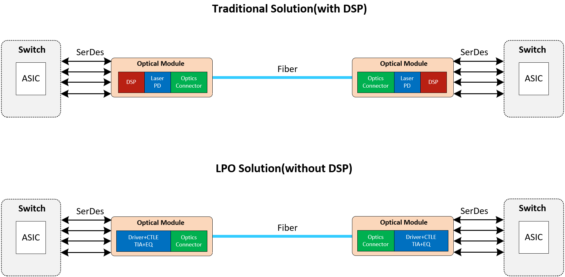
Figure 1: Traditional Solution with DSP vs. LPO Solution without DSP
Traditional high-speed optical modules rely heavily on Digital Signal Processors (DSPs) and Clock Data Recovery (CDR) circuits to perform signal equalization, retiming, and compensation during high-speed data transmission. While DSPs significantly improve signal quality, they also introduce additional latency and consume considerable power.
LPO takes a different approach by implementing a pure analog optical link. Instead of performing signal processing inside the optical module, the responsibility for equalization and signal correction is shifted to the host-side SerDes within GPUs, switches, or NICs.
In a typical LPO architecture:
-
The transmitter uses a high-linearity driver IC to directly drive the optical modulator, converting electrical signals into optical signals.
-
The receiver performs optical-to-electrical conversion and amplification using a high-linearity transimpedance amplifier (TIA).
-
Signal equalization and compensation are handled by the SerDes (Serializer/Deserializer) on the host-side xPU, which places higher requirements on the analog signal processing capability of the host device.
Key Advantages of LPO
Low Power Consumption: Removing the DSP can reduce module power consumption by approximately 30–50%, while also lowering signal processing latency. Compared with traditional DSP-based solutions, overall power consumption can be reduced by more than 50%.
Lower Cost: DSP chips represent a significant portion of the BOM (Bill of Materials) cost, accounting for roughly 20–40% of the module cost. Eliminating the DSP effectively removes this cost. Although integrating equalization functions into drivers and TIAs slightly increases their cost, the overall expenditure is still reduced.
Ultra-Low Latency: LPO eliminates the DSP processing stage, reducing signal processing steps and therefore minimizing transmission latency. This advantage is particularly valuable in high-performance computing (HPC) environments where latency directly impacts system performance.
By removing the DSP from the optical module, LPO creates a pure analog transmission path, significantly reducing power consumption and latency, making it an important direction for next-generation high-bandwidth, energy-efficient data center interconnects.
Challenges of LPO
Despite its advantages in power consumption and latency, LPO still faces several technical and ecosystem challenges in practical deployment.
Limited Transmission Distance: Without DSP-based equalization and error correction, LPO links may experience higher bit error rates (BER) and shorter supported transmission distances. Continuous optimization in link design, signal integrity, and error control mechanisms is required to mitigate these limitations.
Lack of Standardization and Interoperability: LPO standardization is still in its early stages. Compatibility between vendors is not yet fully mature, and current deployments are better suited to single-vendor ecosystems. In multi-vendor environments, issues such as inconsistent interface definitions and unclear system responsibilities may arise. Until the ecosystem matures, traditional DSP-based solutions still maintain certain advantages.
Electrical Channel Design Challenges: LPO relies heavily on the linearity and analog performance of host-side SerDes. As mainstream signaling speeds evolve from 112G to 224G, existing LPO architectures face new limitations in signal bandwidth and noise control. Maintaining stable link performance at higher speeds remains a key technical challenge for the industry.
NPO: Near-Packaged Optics
What Is NPO?
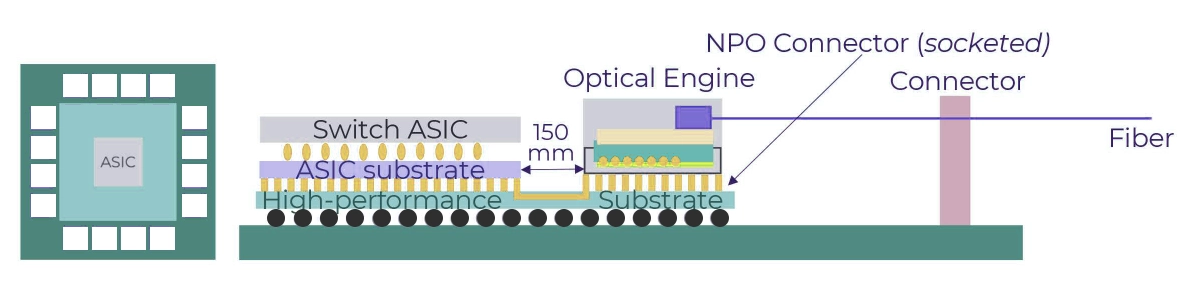
Near-Packaged Optics (NPO) is a highly integrated optical interconnect solution positioned between traditional pluggable optical modules and CPO.
Figure 2: NPO (Near-Packaged Optics) Architecture
The core concept of NPO architecture is to place the optical engine and xPU chips (such as GPUs, NPUs, or switch ASICs) side by side on the same high-performance PCB or organic substrate, connected through extremely short high-speed electrical traces.
The distance between the GPU and the optical engine is typically kept within a few centimeters, and channel loss can be maintained below 13 dB, significantly improving signal integrity and bandwidth utilization.
Key Advantages of NPO
High Bandwidth with Low Signal Loss: Because the signal path is very short, attenuation and crosstalk during transmission are significantly reduced. High-bandwidth transmission can be achieved without relying on complex DSP compensation. Typical systems support 800G and higher data rates, providing improved signal integrity.
Improved Thermal Design: Unlike CPO, the optical engine and xPU in NPO are separately packaged. Optical components are not directly exposed to the high thermal environment of GPU cores, avoiding wavelength drift and performance fluctuations. Independent thermal management structures make it easier to control temperature distribution and enable more flexible thermal designs.
Easy Maintenance and Replaceability: The optical engine is packaged as an independent module. If an optical component fails, only the optical engine needs to be replaced rather than the entire GPU or switch chip. This design significantly reduces maintenance complexity and operational costs, improving overall system serviceability.
Challenges of NPO
Limited Integration Density: Although NPO significantly improves integration compared to traditional solutions, electrical interconnections still require substrate routing. As a result, the overall integration density remains lower than that of CPO, making it difficult to achieve the shortest possible transmission path.
Limited Optimization for Bandwidth Density and Power: At higher transmission speeds such as 1.6T or 3.2T, electrical interconnect losses and power consumption increase. Improvements in materials, routing technologies, and interface standards will be required to further enhance energy efficiency.
Latency Control: Although latency is significantly reduced compared to traditional optical modules, large-scale interconnect systems still require careful balancing of signal delay and link uniformity to ensure system-level synchronization.
Overall, NPO achieves a practical balance between bandwidth, power efficiency, and maintainability, making it a realistic solution in today's optical interconnect ecosystem. It alleviates the physical limitations of traditional pluggable modules while avoiding the packaging complexity introduced by CPO, positioning itself as an important transitional architecture for AI and HPC clusters moving toward optical interconnects.
CPO: Co-Packaged Optics
What Is CPO?
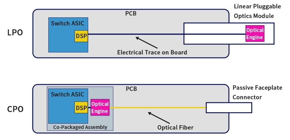
Co-Packaged Optics (CPO) is a highly integrated optoelectronic interconnect technology evolved from NPO. The core concept is to directly integrate the optical engine with a switch ASIC or compute chip (xPU) within the same package.
This design eliminates traditional pluggable optical modules connected via front-panel interfaces and shortens the electrical transmission path from several centimeters to millimeter-level distances, significantly reducing signal attenuation, power consumption, and latency.
In conventional architectures, electrical signals must travel across relatively long PCB traces before reaching optical modules, leading to insertion loss and crosstalk issues that limit system interconnect density.
CPO integrates optical engines and electrical chips onto a silicon interposer or organic interposer, enabling millimeter-scale interconnects and fundamentally improving signal integrity and bandwidth efficiency. This packaging approach represents the evolutionary direction toward ultimate integration in optical interconnect technologies.
Figure 3: LPO vs. CPO Architecture
Notably, the development of silicon photonics technology is closely tied to the evolution of CPO. Silicon photonics provides highly integrated, low-power, and cost-effective optical engine solutions, forming a key foundation for the rapid advancement of CPO.
Basic Structure of a CPO System
A CPO system typically includes electrical chips (ASICs or GPUs), optical engines, silicon interposers, and fiber interfaces.
Transmitter: High-speed electrical signals generated by the SerDes inside the electrical chip are transmitted through micro-bump interconnects on the interposer directly to the optical engine. A driver IC then drives the optical modulator to complete electro-optical conversion, and the optical signal is transmitted through optical fibers.
Receiver: Incoming optical signals are converted into electrical signals by photodetectors, amplified by TIAs, and transmitted back to the electrical chip via micro-bump interconnects for signal decoding.
Interconnect Path: The entire electro-optical conversion path is only a few millimeters long, significantly reducing transmission distance, channel loss, and system complexity.
CPO Packaging Types
Based on packaging depth, CPO can be classified into three forms:
Type A (2.5D Packaging): The optical engine and ASIC are mounted on the same package substrate, with electrical connection lengths around 10 cm or less.
Type B (Advanced 2.5D Chip Packaging): Wafer-level packaging technology is used to improve packaging density and signal transmission efficiency.
Type C (3D Packaging): Achieves vertical stacking of optoelectronic chips, shortening the interconnect path to millimeter levels. This represents the highest level of integration in CPO architectures.
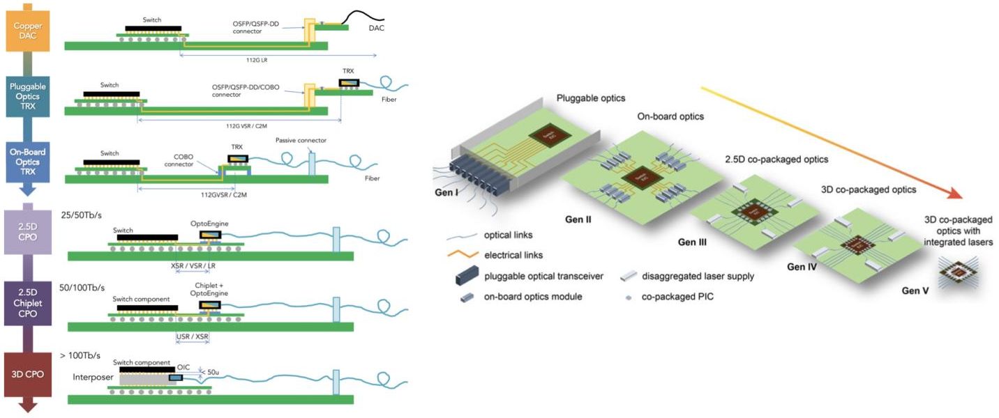
Figure 4: Evolution of data center interconnect architectures, showing the transition from copper connections and pluggable optics to more advanced optical integration technologies such as on-board optics, co-packaged optics (CPO), and 3D co-packaged optics.
Key Advantages of CPO
High Bandwidth and Low Power: Due to extremely short electrical paths, CPO can support 1.6T to 3.2T per port high-speed interconnects while significantly improving signal integrity and transmission speed. According to Broadcom, CPO systems can reduce power consumption by more than 50%, with typical energy efficiency improving from 15–20 pJ/bit to 5–10 pJ/bit.
High Interconnect Density and Space Efficiency: By integrating optical engines into the package, front-panel space can be freed, significantly increasing I/O density in switches and GPU systems while providing more expansion capacity for high-performance computing platforms.
Low Latency and High Reliability: CPO eliminates intermediate electrical connections and DSP compensation stages, shortening latency paths and reducing sensitivity to electromagnetic interference (EMI), thereby improving signal stability.
Superior System Energy Efficiency: The highly integrated packaging architecture reduces conversion losses and optimizes overall data center PUE (Power Usage Effectiveness), making it ideal for AI training clusters and hyperscale switching platforms.
Challenges of CPO
Despite its performance and efficiency advantages, CPO still faces several challenges in manufacturing and maintenance.
High Packaging Complexity: Optoelectronic co-packaging places extremely high demands on thermal management, mechanical stability, and manufacturing yield, leading to higher production costs compared with traditional optical module solutions.
Limited Serviceability: Because optical engines and ASICs are tightly integrated, failures in optical components may require replacing the entire package, increasing maintenance complexity.
Immature Ecosystem: CPO requires new standards for optoelectronic packaging, testing systems, and automated manufacturing processes. The industry ecosystem is still in an early stage of development.
LPO vs. NPO vs. CPO: What Are the Differences?
| Technology |
Architecture |
Electrical Distance |
Power Efficiency |
Latency |
Maintainability |
Typical Use Case |
| LPO |
Pluggable optics without DSP |
Long electrical path |
High |
Low |
Easy |
AI clusters, HPC networking |
| NPO |
Optical engine near compute chip |
Few centimeters |
Very high |
Very low |
Replaceable |
AI accelerators, switch systems |
| CPO |
Optical engine co-packaged with ASIC |
Millimeter-level |
Extremely high |
Ultra-low |
Difficult |
Future hyperscale AI clusters |
Optical Interconnect Roadmap: From 800G to 3.2T
Today, 800G optical transceivers are widely deployed in modern AI data centers to support high-performance GPU networking.
As AI clusters continue to scale, the industry is moving toward 1.6T optical modules and future 3.2T interconnect technologies, which will require more advanced optical integration methods such as NPO and CPO.
Silicon photonics will play a critical role in this transition by enabling high-density optical integration with lower power consumption and improved scalability.
Conclusion
As AI and high-performance computing data centers continue to evolve toward hyperscale architectures and higher compute densities, optical interconnect technologies are gradually shifting from pluggable modules to package-level integration.
-
LPO provides a practical low-power, low-latency solution for short-distance high-performance scenarios.
-
NPO achieves a balance between bandwidth density and maintainability through near-package optical placement.
-
CPO pushes interconnect performance to its limits through co-packaged integration, forming a critical foundation for future 1.6T and beyond high-speed interconnects.
Each architecture emphasizes different design priorities, and together they form the technological framework for optical interconnects in next-generation AI data centers.
Recommedned Reading:
 English